- 您现在的位置:买卖IC网 > Sheet目录489 > NTHD4P02FT1G (ON Semiconductor)MOSFET P-CH 20V 2.2A CHIPFET
NTHD4P02F
Power MOSFET and
Schottky Diode
?20 V, ?3.0 A, Single P?Channel with
3.0 A Schottky Barrier Diode, ChipFET t
Features
http://onsemi.com
? Leadless SMD Package Featuring a MOSFET and Schottky Diode
? 40% Smaller than TSOP?6 Package with Similar Thermal
Characteristics
? Independent Pinout to each Device to Ease Circuit Design
? Ultra Low V F Schottky
? Pb?Free Package is Available
V (BR)DSS
?20 V
MOSFET
R DS(on) TYP
?130 m W @ ?4.5 V
200 m W @ ?2.5 V
SCHOTTKY DIODE
I D MAX
?3.0 A
Applications
? Li?Ion Battery Charging
? High Side DC?DC Conversion Circuits
? High Side Drive for Small Brushless DC Motors
? Power Management in Portable, Battery Powered Products
V R MAX
20 V
S
V F TYP
0.510 V
A
I F MAX
3.0 A
MOSFET MAXIMUM RATINGS (T J = 25 ° C unless otherwise noted)
G
Parameter
Symbol
Value
Units
Drain?to?Source Voltage
Gate?to?Source Voltage
V DSS
V GS
?20
± 12
V
V
D
P?Channel MOSFET
C
SCHOTTKY DIODE
Continuous Drain
Current
Steady
State
T J = 25 ° C
T J = 85 ° C
I D
?2.2
?1.6
A
ChipFET
Pulsed Drain
Current
t v 5s T J = 25 ° C
t p = 10 m s
I D
I DM
?3.0
?9.0
A
A
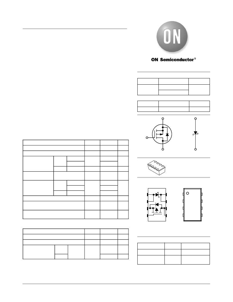
CASE 1206A
STYLE 3
Power Dissipation
Steady
State
T J = 25 ° C
T J = 85 ° C
P D
1.1
0.6
W
PIN CONNECTIONS
MARKING
DIAGRAM
t v 5s
T J = 25 ° C
2.1
A
1
8
C
1
8
Continuous Source Current (Body Diode)
Operating Junction and Storage
Temperature
Lead Temperature for Soldering Purposes
(1/8 ″ from case for 10 s)
I S
T J , T STG
T L
?2.1
?55 to 150
260
A
° C
° C
A
S
G
2
3
4
7
6
5
C
D
D
2
3
4
7
6
5
SCHOTTKY DIODE MAXIMUM RATINGS
(T J = 25 ° C unless otherwise noted)
Parameter
Peak Repetitive Reverse Voltage
DC Blocking Voltage
Symbol
V RRM
V R
Value
20
20
Units
V
V
C3 = Specific Device Code
M = Month Code
G = Pb?Free Package
ORDERING INFORMATION
Average Rectified
Forward Current
Steady
State
t v 5s
T J = 25 ° C
I F
2.2
3.0
A
A
Device
NTHD4P02FT1
NTHD4P02FT1G
Package
ChipFET
ChipFET
Shipping ?
3000/Tape & Reel
3000/Tape & Reel
Maximum ratings are those values beyond which device damage can occur.
Maximum ratings applied to the device are individual stress limit values (not
normal operating conditions) and are not valid simultaneously. If these limits are
exceeded, device functional operation is not implied, damage may occur and
reliability may be affected.
(Pb?free)
?For information on tape and reel specifications,
including part orientation and tape sizes, please
refer to our Tape and Reel Packaging Specifications
Brochure, BRD8011/D.
? Semiconductor Components Industries, LLC, 2005
November, 2005 ? Rev. 7
1
Publication Order Number:
NTHD4P02F/D
发布紧急采购,3分钟左右您将得到回复。
相关PDF资料
NTHD5903T1G
MOSFET PWR P-CH DUAL20V CHIPFET
NTHD5904NT1G
MOSFET N-CHAN 3.3A 20V CHIPFET
NTHS2101PT1
MOSFET P-CH 8V 5.4A CHIPFET
NTHS4101PT1G
MOSFET P-CH 20V 4.8A CHIPFET
NTHS4166NT1G
MOSFET N-CH 30V 4.9A CHIPFET
NTHS4501NT1G
MOSFET N-CH 30V 4.9A CHIPFET
NTHS5404T1G
MOSFET N-CH 20V 5.2A CHIPFET
NTHS5441T1G
MOSFET PWR P-CH 3.9A 20V CHIPFET
相关代理商/技术参数
NTHD5902T1
功能描述:MOSFET 2N-CH 30V 2.9A CHIPFET RoHS:否 类别:分离式半导体产品 >> FET - 阵列 系列:- 产品目录绘图:8-SOIC Mosfet Package 标准包装:1 系列:- FET 型:2 个 N 沟道(双) FET 特点:逻辑电平门 漏极至源极电压(Vdss):60V 电流 - 连续漏极(Id) @ 25° C:3A 开态Rds(最大)@ Id, Vgs @ 25° C:75 毫欧 @ 4.6A,10V Id 时的 Vgs(th)(最大):3V @ 250µA 闸电荷(Qg) @ Vgs:20nC @ 10V 输入电容 (Ciss) @ Vds:- 功率 - 最大:1.4W 安装类型:表面贴装 封装/外壳:PowerPAK? SO-8 供应商设备封装:PowerPAK? SO-8 包装:Digi-Reel® 产品目录页面:1664 (CN2011-ZH PDF) 其它名称:SI7948DP-T1-GE3DKR
NTHD5902T1/D
制造商:未知厂家 制造商全称:未知厂家 功能描述:Power MOSFET Dual N-Channel ChipFET?
NTHD5903T1
功能描述:MOSFET -20V -3A Dual RoHS:否 制造商:STMicroelectronics 晶体管极性:N-Channel 汲极/源极击穿电压:650 V 闸/源击穿电压:25 V 漏极连续电流:130 A 电阻汲极/源极 RDS(导通):0.014 Ohms 配置:Single 最大工作温度: 安装风格:Through Hole 封装 / 箱体:Max247 封装:Tube
NTHD5903T1/D
制造商:未知厂家 制造商全称:未知厂家 功能描述:Power MOSFET Dual P-Channel ChipFET?
NTHD5903T1_05
制造商:ONSEMI 制造商全称:ON Semiconductor 功能描述:Power MOSFET -20 V, -3.0 A, Dual P-Channel ChipFET
NTHD5903T1-D
制造商:ONSEMI 制造商全称:ON Semiconductor 功能描述:Power MOSFET Dual P-Channel ChipFET
NTHD5903T1G
功能描述:MOSFET -20V -3A Dual P-Channel RoHS:否 制造商:STMicroelectronics 晶体管极性:N-Channel 汲极/源极击穿电压:650 V 闸/源击穿电压:25 V 漏极连续电流:130 A 电阻汲极/源极 RDS(导通):0.014 Ohms 配置:Single 最大工作温度: 安装风格:Through Hole 封装 / 箱体:Max247 封装:Tube
NTHD5904N
制造商:ONSEMI 制造商全称:ON Semiconductor 功能描述:Power MOSFET 20 V, 4.5 A, Dual N−Channel, ChipFET
